- Silicon PhotonicsSilicon PhotonicsThanks to the immense transmission capacity and low energy consumption, optical communication is penetrating ever deeper layers of data/communication networks. Servers are increasingly connected via glass fibers, peripherals are starting to leverage photonic cables that combine high capacity and convenient lengths, and soon computers will see internal functionalities transferred to the medium of light in form of integrated photonic circuits (PICs). The important new field of silicon photonics requires that these new components must be tested and assembled with the highest precision since a misalignment would mean lost yield, poor performance or failure.
- Technology of Active AlignmentTechnology of Active AlignmentThe development and manufacturing of photonic devices reminds us in many ways of the early years of the semiconductor industry in the mid-1980s. PI was a young company at the time and already deeply integrated into the production tools being deployed in early fabs around the world. But these tools were usually homemade by in-house or captive local systems integrators. The vast ecosystem of toolmakers that the industry enjoys today had yet to be born. The situation is similar in photonics today: the toolmaker ecosystem is just emerging. While the front-end manufacturing of photonic-enabled wafers can rely on the existing microlithography infrastructure, the industry for the back-end processes is just starting to develop. Some excellent tools and toolmakers have already emerged, and in-house test/assembly machine design remains an option for many silicon photonics device manufacturers.
- The Missing LinkThe Missing LinkAs an example of the fresh innovations emerging for photonics-device assembly, TEGEMA B.V. (NL), the multidisciplinary system integrator, has developed a modular machine platform for the automated assembly of optical components, in particular of photonically integrated circuits (PICs). The system, which works with submicron precision, can grow from tasks in research and development of PICs up to their series production thanks to its intelligent architecture.
- SiPh Wafer ProbingSiPh Wafer ProbingThe integration of photonic structures or elements on a silicon chip presents, already at wafer level, a multitude of new challenges for the testing technology of these elements. In order to transmit the design of the structure, from the concept through its qualification up to series production, a very large amount of performance data of the respective element is required.
- Technology of Active Alignment
- MicroscopyMicroscopyMicroscopy, like no other technology, is constantly expanding our knowledge about what holds the world together at its core, about what the building blocks of life look like. In life sciences, materials research, geology, archeology, mineralogy... again and again, microscopes in the hands of brilliant researches provide the newest findings and so make innovations possible.
- Configure your Microscope StageConfigure your Microscope StageThe precise and fast movement of the sample or the objective play a crucial role for achieving good results when working with light microscopes. The demands on stages and scanners are manifold. In addition to the position resolution, which directly correlates with the optical resolution of the microscope, velocity and dynamics are other elemental requirements for the motion system.
- Open Source Microscopy ProjectsOpen Source Microscopy ProjectsMicroscopy is one of the technologies that is constantly reinventing itself. The first microscopes from the early 17th century were very simple in design, but countless developments have steadily increased their performance.
- Electron MicroscopyElectron MicroscopyApplications for electron microscopy cover a broad spectrum from semiconductor inspection through materials research to molecular biology research. In conventional TEM as well as in the newer Cryo-TEM, which was awarded the Nobel Prize in 2017, the samples have to be nanopositioned with high precision in an XYZ coordinate and then tilted around one axis to produce a certain number of transmission images for image reconstruction.
- Atomic Force MicroscopyAtomic Force MicroscopyAtomic force microscopy supplies researchers and developers extremely high resolution topographical data from a large number of different minerals, polymers, mixtures, composite materials or biological tissue. This technology, developed in the 1980s, enables users to obtain subatomic resolved images of sample surfaces.
- Configure your Microscope Stage
- BiotechnologyBiotechnologyBiotechnology is one of the oldest applied sciences of humanity: Using yeast to bake bread or to ferment fruit to alcohol is, for example, biotechnology that is being practiced and developed for thousands of years. Today, this discipline has countless applications in medicine (red), agriculture (green), and the industry (white).
- Genome SequencingGenome SequencingBlue, brown, or green eyes? Which hair color? Which illnesses may affect us? Whose child am I? All of this information and much more is stored, or at least set, in our genes. In crime novels, but also in real life, genetic analysis is called upon for advice when it comes to finding an answer to the question, "Who did it?". The "genetic fingerprint" has become an often consulted and unmistakable evidence. Last but not least, genome analysis holds the key to groundbreaking discoveries for many health-related questions.
- Genome Sequencing
- Medical DevicesMedical DevicesProgress in medical research, diagnostics, and therapy requires high-performance, precise motion and positioning systems. High positioning precision, compact dimensions, low energy consumption, speed, and absolute reliability are just some of the requirements for the drives in use. However, the applications are so varied as are the technologies and solutions with which PI supports its customers on all levels of value creation: From operation robots through miniature drives for endoscopy cameras to aperture adjustment in radiotherapy or even the precise, targeted positioning of patients on operating tables that can be adjusted in six degrees of freedom.
- EndoscopyEndoscopyModern medical technology focuses on developing therapies that cause as little discomfort to patients as possible. Endoscopes that allow minimally invasive surgery, make an important contribution to this, for example, in laparoscopy. Especially during medical interventions, the demand for focused and detailed image information is of the highest priority in order to achieve the best possible chances of success.
- Surgical Robots: Patient Couch for RadiotherapyPatient Couch for RadiotherapyIn radiotherapy, it is particularly important to ensure that healthy tissues are protected. This is why, it is absolutely necessary to position the patient precisely during radiotherapy. Patient couches that employ hexapods from PI are very well suited for this task.
- Endoscopy
- AstronomyAstronomyEven in the earliest history, humans were incredibly fascinated by space; cave paintings or the Nebra sky disk bear witness of this. The question, "What are those shimmering colors in the night sky?" developed into the question of how galaxies, stars, and planetary systems developed. Highly sensitive systems such as the Atacama Large Millimeter/Submillimeter Array telescope assembly – in short ALMA – provide the data with which researchers are trying to solve these mysteries – and raise new questions.
- ALMA-ArrayALMA-ArrayA spectacular, albeit essentially impossible image caused a worldwide sensation on April 10, 2019: The first ever "photograph" of a black hole. 55 million light years away at the center of the M87 galaxy. The unbelievably strong gravitational pull means that even light cannot escape. But, thanks to the Event Horizon Telescope - a combination of eight radio telescopes - the participating researchers outsmarted physics to a certain extent and for the first time, created an image of a black hole's shadow. This shadow is cast by the radiation from the distorted light while being irrevocably absorbed by the black hole.
- ALMA-Array
- SemiconductorSemiconductorFor decades, no other product has shaped and changed our lives as much as the omnipresent microchips. Whether computers in all their variants, cell phones and smartphones, game consoles, cars and airplanes, yes, now even the home refrigerator, oven or iron and toaster – nothing works anymore without these jack-of-all-trades made of doped silicon. PI has played a large part in this success story.
- Search
In the CM300xi SiPh wafer probing station from FormFactor, PI's F-712.HA2 double-sided fiber alignment system actively aligns signal-carrying glass fibers to photonic structures on silicon photonic wafers The integration of photonic structures or elements (e.g. waveguides, laser and photodiodes, multiplexer) on a silicon chip presents, already at wafer level, a multitude of new challenges for the testing technology of these elements. In order to transmit the design of the structure, from the concept through its qualification up to series production, a very large amount of performance data of the respective element is required.
When taking into account the high process cost up until when the SiPh chip is finally packaged, faulty chips should be identified early on so that they can be removed from the ongoing manufacturing process.
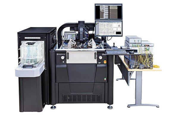
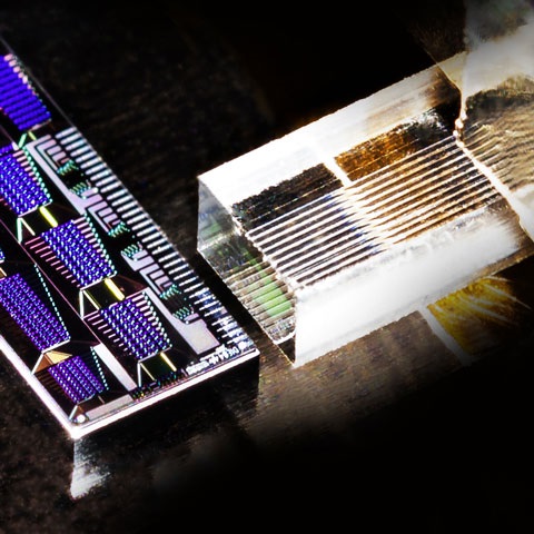
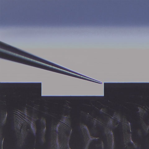
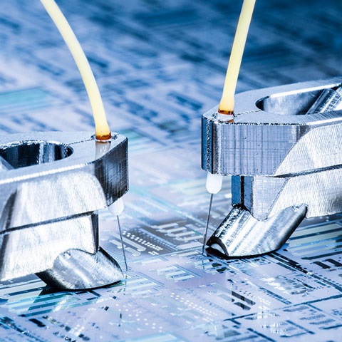
For an effective and efficient implementation of this task, FormFactor has developed fully-automated SiPh wafer probers. Many process steps employed here, follow established standards in the semiconductor industry. However, for testing the functionality and quality of photonic structures, the optical properties must also be tested. For this purpose, signal-carrying glass fibers must be aligned with high precision to the photonic element to be tested. The alignment must be made in six degrees of freedom (for both, shifts and rotations) since the test only delivers conclusive information with an optimal optical power coupling. In the SiPh wafer probers from FormFactor, PI's Fast Multi-Channel Photonics Alignment-System (FMPA) takes on this central task.
Sophisticated Alignment Process
The alignment process is subject to a series of highly challenging requirements. In particular:
- Maintaining the optimum distance between the probe (glass fiber) and photonic structure in order to minimize the loss of signal and to ideally simulate the operating conditions
- Aligning in all six degrees of freedom in order to best superimpose the optical axis of the structure to be tested with the test fiber
- Optimizing the position in the shortest time
- Avoiding a physical contact between the probe and the wafer at all costs
The initial goal of the listed requirements is to be able to react with high flexibility to differing chip designs. Edge emitters, for example, require a horizontal alignment of the test fiber, whereas grating couplers require a vertical alignment at wafer level. With the alignment on edge emitters, testing at die-level also becomes possible.
The best coupling efficiency for applications with high bandwidth can be reached if fibers / arrays (right) are placed as close as possible to the exposed waveguide facets by the horizontal die-level edge coupling. The real edge coupling makes an exact simulation of real-life conditions possible, which come very close to the actual application The high speed of the alignment process is a further important goal for achieving an economical series production of SiPh components. Thousands of photonic structures are present on a wafer. The faster the alignment of the signal-carrying glass fibers, the faster and, therefore, more economical the test. The FMPA systems from PI position glass fibers and photonic structures in FormFactor's silicon photonic wafer probers in a fraction of a second. This makes the testing of a wafer in hours or a few days possible, instead of conventionally taking weeks or even months.
Despite the speed and precision, it is absolutely necessary to avoid a direct contact between the probe and wafer. Behind this requirement, the goal is to avoid direct damage to chip structures and the formation of particles. For this purpose, sensor technologies from PI are also being employed.
- Search