Positioning Solutions for Improving Throughput and Enabling the Next Technology Node in Semiconductor Manufacturing
Today, semiconductor technology represents one of the most important industry sectors in the world. It paves the way for progress made in processor technology, data storage, signal processing, and opto-electronics and, therefore, facilitates for the next generation of microprocessors, memory chips, and power semiconductors. These semiconductor components are the prerequisite for essential developments in 6G technology, Internet of Things (IoT), Cloud and Edge Computing, or Electric and Autonomous Vehicles. At the same time, these growing markets are placing high demands on semiconductor manufacturers: Even smaller and more complex integrated circuits (IC) with higher functional density and reduced energy consumption, shorter product and technology innovation cycles, higher volumes, and increasing cost pressure.
Each equipment component and machine used by integrated device manufacturers (IDMs) or foundry companies for the manufacturing of semiconductor chips must follow these requirements. And also each of the demanding and sensitive manufacturing steps – both in the development of process-related technologies and the numerous processing steps a silicon wafer undergoes.
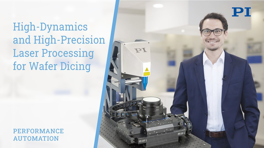
Lithography is one of the most decisive process steps in wafer processing. This is where the foundation for the functionality of the chips is laid, i.e., processor speed, storage capability, space requirements, and power consumption. During the repetitive exposure process, smallest structures for printed circuit boards, transistors, and other components have to be transferred onto the silicon wafer.
Measurement and inspection processes are necessary at all critical points in the manufacturing process to ensure high quality and reliability of the final products and also the yield of the cost-intensive chip production.
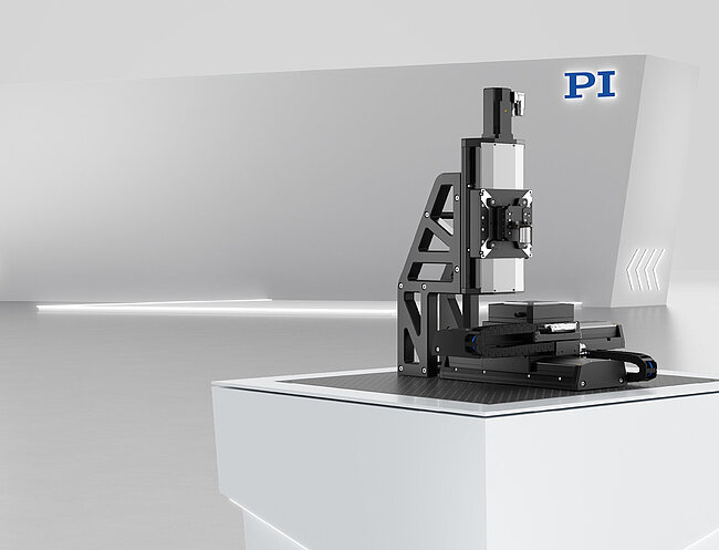
In many manufacturing steps, the ability to move components with nanometer and even sub-nanometer precision and with high dynamics, or to hold a position precisely over an extended period of time, plays a crucial role.
PI Supports Semiconductor Equipment Suppliers Worldwide with High-Precision and Reliable Motion and Control Solutions for Applications Such As:
PI also offers positioning solutions outside of the actual production process, for example, for equipment in technology development, in the qualification of tools, for repairing masks, or for the production of test probe cards.
PI offers 50 years of experience in piezo technology and nanopositioning, a broad technological range, and a high vertical range of manufacturing in order to be able to develop and provide components and systems that are optimally adapted to the respective process: From sensors, piezo actuators as well as systems and motors through air bearing motion systems with linear motor drives up to controllers, drive modules, software, and firmware.
In addition, the EtherCAT®-based >> motion controller and drive solutions from ACS, a subsidiary of PI, enable flexible and high-precision control of complex multi-axis systems for use in semiconductor manufacturing. For example, by employing intelligent gantry controls or servo control for subnanometer standstill jitter.
As a long-standing supplier to semiconductor equipment manufacturers, PI understands the requirements of the semiconductor industry and works closely with its customers right from the design phase to select solutions that can meet current requirements and support future technological trends and technology nodes.
With individual service level agreements (SLA) and global service hubs, PI is also able to respond to requirements at short notice and thus support reliable process performance. Due to the high quality and reliability of the components and systems – based on extensive long-term tests, manufacturing in cleanrooms with the highest cleanliness standards and a Copy Exactly Strategy – PI provides its customers high availability of the solutions.