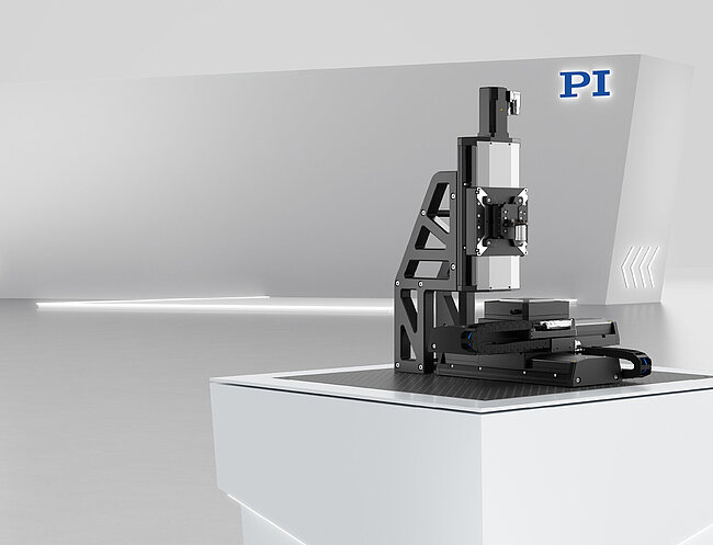
The Fast Lane to a Precision Advantage
In almost all industrial manufacturing processes, the correct positioning of individual components and their precise alignment to each other are essential for proper product function and manufacturing efficiency. This is even more important as products and their components get smaller and smaller. This ongoing process of miniaturization makes alignment more challenging and more expensive. With 50 years of experience in nanopositioning, hundreds of patents, and expert staff, PI has helped countless customers successfully master the challenge of nanopositioning and gain a decisive competitive advantage.
Let us guide you to "the fast lane to a precision advantage".
Your Advantages with PI as a Partner
Setting the pace in nanopositioning
For 50 years, PI has kept pushing the boundaries of nanopositioning.
Extensive patent portfolio
A large patent portfolio ensures our customers‘ competitive advantage.
Broad technology pipeline
We offer our customers access to a full and constantly evolving
technology pipeline.
technology pipeline.
Passionate advice
Delivering competent advice and solutions runs deep in our DNA. This unique foundation is built on many years of experience, passion and teams of highly qualified developers and application specialists.
Preferred source for science and research
Scientists from all disciplines prefer nanopositioning solutions from PI. Our products are cited ten times more frequently in scientific publications than competitive products.
Lots of testimonials
There is countless proof of performance from
semiconductor technology to
photonics to life sciences to
microscopy and
mechanical engineering.
semiconductor technology to
photonics to life sciences to
microscopy and
mechanical engineering.